If you’ve ever held a phone, flicked on a smart bulb, or hopped into a modern car, you’ve touched a global supply chain that quietly runs on silicon. For decades, production of those tiny, crucial chips was dominated by East Asia—Taiwan, South Korea, parts of China. India, meanwhile, mostly assembled finished electronics and imported the core components. That’s changing—fast.
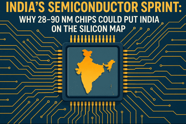
Over the past few years, India has kicked off a serious, industry-wide push: fabs (fabrication plants) to make chips, OSAT/ATMP plants to assemble and test them, and policy programs to fund the entire pipeline. The exciting (and pragmatic) twist? India’s first wave is not chasing the world’s most extreme nodes like 2–3 nm; we’re starting where the market is enormous and chronically under-served: 28–110 nm and adjacent “legacy” technologies. These are the chips that keep cars braking safely, lights turning on, routers humming, and factories running. And demand for them isn’t going away.
Before we dive into timelines and technology, let’s set expectations. We’ll keep this article grounded in what’s real today—who’s building what, where, and when—then look ahead to how India can climb the node ladder. Where needed, I’ll point out uncertainties so your mental model stays honest. Ready? Let’s roll.
1) Why 28–90 nm Is a Smart Starting Line
Let’s begin with a truth the headlines rarely celebrate: most of the world’s chips are not 3 nm or 2 nm. The cutting-edge system-on-chip (SoC) inside your flagship phone may be—but it’s surrounded by dozens of support chips that don’t need such extremes. Power management ICs, display drivers, motor controllers, sensors, microcontrollers for appliances and cars—these typically live in older, mature nodes. During the 2020–2022 chip crunch, automakers didn’t stall because they lacked 3 nm Apple-class processors; they stalled because they couldn’t source basic controllers and analog/power chips in time. Demand for these “workhorse” semiconductors is persistent and huge.
That’s exactly why India’s first fabs are targeting 28–110 nm classes: you can build a reliable domestic base where global demand is steady, learn at industrial scale, and reduce import dependence across critical sectors (automotive, energy, industrial, defense, telecom). Then, on top of this base, you can train talent, stabilize yields, and take measured steps toward smaller geometries. It’s chess, not checkers.
2) What India Is Actually Building: Plants, Partners, and Places
So what’s on the ground—and what’s coming? Here are the headline projects that define India’s new silicon landscape.
Tata Electronics + PSMC (Dholera, Gujarat) — India’s First Fab
The Government of India approved Tata Electronics (TEPL) to build a semiconductor fabrication facility in Dholera, in partnership with Taiwan’s Powerchip Semiconductor Manufacturing Corporation (PSMC). Investment is ~₹91,000 crore (~US$11 billion). Construction begins with targeted capacity around 50,000 wafers/month at mature nodes (28–110 nm range) serving power, analog, display drivers, and automotive MCUs. This is a foundational plant—India’s first true “fab.”
Why it matters: A domestic fab means India isn’t just assembling chips—it’s making them. That reduces supply risk for everything from EVs to smart meters—and trains an entire generation of process engineers and technicians.
Micron ATMP/OSAT (Sanand, Gujarat) — Memory Assembly & Test
Micron Technology is setting up a large assembly, test, and packaging facility (ATMP) in Sanand. Phase-1 includes ~500,000 sq ft of cleanroom space, with phased ramp-up aligned to global demand. This is primarily for memory (think DRAM, NAND used in SSDs and phones). Phase-1 targeted late-2024 ops, with further scaling mid-decade.
Why it matters: Memory packaging anchors a different segment of the value chain and complements logic fabs. It also builds vendor ecosystems—substrates, molding compounds, handlers, and reliability labs.
CG Power + Renesas + Stars (Sanand, Gujarat) — OSAT for “Specialized Chips”
A joint venture of CG Power (Murugappa Group) with Japan’s Renesas and Thailand’s Stars Microelectronics is building an OSAT facility in Sanand with ~₹7,600 crore investment. The JV roadmap spans legacy QFN/QFP to advanced FC-BGA/CSP packaging, ultimately ramping to ~15 million units/day (per JV note). Focus markets include automotive, consumer, industrial, and 5G.


Why it matters: OSAT capacity is the bloodstream of the chip world. You can fabricate anywhere; without robust packaging/test, chips don’t ship.
HCL + Foxconn (Jewar/Noida, Uttar Pradesh) — Display-Driver OSAT
HCL and Foxconn (Hon Hai) have a Cabinet-approved OSAT JV in Jewar (near Noida International Airport), focusing on display driver ICs (DDIs) for phones, laptops, automotive clusters, and more. Planned capacity is ~20,000 wafers/month, with ~36 million DDIs/month output once mature. Commercial production has been reported as targeting 2027.
Why it matters: DDIs are the unsung heroes behind every screen. Localizing them supports India’s display, smartphone, and auto electronics ecosystems.
Ecosystem Signals: Equipment, Materials, and Support
Even equipment majors are positioning for India: Tokyo Electron (a top fab-tool maker) set plans to open offices in Dholera and Assam to support Tata Electronics’ fab and assembly initiatives—an early indicator that upstream suppliers are aligning for Indian volume.
So far, so good—we’ve mapped the core pieces of India’s first semiconductor stack: front-end fab at Dholera, multiple ATMP/OSATs at Sanand and Jewar, and the suppliers beginning to cluster nearby. Let’s move to the policy engine powering this push.
3) The Policy Engine: India Semiconductor Mission (₹76,000 crore)
In 2021, the Union Cabinet approved the India Semiconductor Mission (ISM) with an outlay of ₹76,000 crore to catalyze fabrication, display manufacturing, and chip design. The program bundles fiscal support, technology-transfer incentives, and project-by-project evaluation—aimed at building fabs, display fabs, ATMP/OSAT, and design ecosystems across states. As of mid-2025, the government has highlighted multiple approved units with cumulative investments crossing ₹1.6 lakh crore across six states.
Translation: This isn’t a single plant announcement; it’s a portfolio strategy—front-end, back-end, and design. That balance is what gives an ecosystem staying power.
4) From Design to Device: How a Chip Becomes a Product (Step-by-Step)
We’ve covered the “who” and “where.” Now, the “how.” The journey from idea to a working chip inside your car or bulb typically looks like this:
Step 1 — System & Chip Architecture
A product company (say, an EV maker) defines functions: motor control, battery management, infotainment. Chip designers map these to silicon blocks—CPU cores, analog IP, memory, I/O.
Step 2 — RTL Design & Verification
Engineers write Register Transfer Level code (Verilog/VHDL) and relentlessly simulate it. This phase weeds out logic bugs before they become expensive mask errors.
Step 3 — Physical Design & Sign-off
Place-and-route tools convert logic into a physical layout. Timing closure, power integrity, clock tree synthesis, and parasitics are hammered into spec. Final checks (DRC/LVS) ensure the layout matches both design rules and intended schematics.
Step 4 — Tape-Out
The validated layout is converted into masks—giant stencils used in the fab’s photolithography systems to pattern silicon.
Step 5 — Fabrication (Front-End: Dholera-class fabs)
Wafers enter months-long journeys through deposition, lithography, etch, ion implantation, and CMP. Mature nodes (28–110 nm) emphasize analog accuracy, power handling, and reliability rather than absolute transistor density.
Step 6 — Assembly, Test, and Packaging (Back-End: Sanand/Jewar)
Known-good dies are cut and packaged—QFN, QFP for cost-effective controllers; FC-CSP/FC-BGA for higher I/O density. Electrical/thermal tests validate every unit. That’s where Micron, CG-Renesas-Stars, and HCL-Foxconn lines come in.
Step 7 — Module Integration & Certification
Chips are mounted on boards, firmware loaded, EMI/EMC and safety certifications run. Only then do they enter the supply chain for cars, appliances, and networks.
Knowing these steps makes the news snippets make sense: fabs without OSAT are bottlenecked, design without packaging yields is academic, and policy without suppliers doesn’t scale. India’s plan is to stand up all three.
5) How India Moves from 90 nm → 28 nm → Single-Digit Nodes (Realistically)
It’s natural to ask: “Why not jump straight to 3 nm?” Because advanced nodes demand enormous capital, decades of know-how, EUV lithography ecosystems, and very high yield discipline. Starting with 28–110 nm builds repeatable muscle memory—process control, contamination management, equipment uptime, and yield learning—at scale. That’s the foundation you need to climb.
Here’s a practical ladder India can climb:
- Stabilize 90–110 nm for analog/power, grow local equipment service, gas/chemical supply, and metrology expertise.
- Ramp 40–65 nm for richer MCUs, connectivity ICs, and mixed-signal SoCs.
- Industrialize 28 nm for display drivers, PMICs, and mid-range logic with better density/power.
- Selective shrink (22/16 nm Planar/FinFET where viable), while expanding compound semiconductors (SiC/GaN) for EV and fast-charging—these aren’t “smaller,” but they’re “harder,” and India’s energy transition needs them.
- Design-first on advanced nodes: even before domestic 3–5 nm fab lines, India can scale chip design on bleeding-edge nodes using foundry partners abroad—and backfill with packaging at home. (India already houses ~20% of the world’s chip design talent, by several government and industry estimates.)
Will India have local 3 nm fabrication by 2030? Official targets and optimism exist; the honest answer is: possible but non-trivial. Don’t under-estimate the value of being the world’s reliable supplier of mature-node chips and advanced packaging first. That alone is a multibillion-dollar, strategically vital niche.
6) What This Means for Automakers, IoT, Telecom, and Energy
Let’s bring this home with real use-cases—because that’s where the payoff lands.
- Automotive (ABS, power steering, ADAS support)
Legacy nodes dominate safety-critical controllers. Local fabs + OSAT shrink lead times and add supply certainty. The 2021–2022 shortages showed how a missing ₹50 controller can halt a ₹10-lakh car. Mature nodes are the backbone of automotive electronics. - Smart Energy & Grids
Smart meters, inverters, and grid controllers lean on robust mixed-signal chips. Domestic availability helps national rollouts and lowers import risk. - 5G/FTTH & Networking
Routers, ONTs, small cells, and power devices use PMICs and RF components that don’t need 3 nm. Packaging advances (FC-CSP) improve thermal and signal integrity. - Consumer & Industrial IoT
Microcontrollers, sensors, and low-power SoCs are overwhelmingly mature-node territory. India’s MSMEs benefit from predictable availability and pricing. - Displays & Mobility
The HCL-Foxconn JV on display drivers directly supports phones, laptops, and vehicle clusters—key for “designed-and-made-in-India” devices.
7) What Students, Startups, and MSMEs Can Do Now (A Practical Playbook)
Before we dive into bullet points, a quick pep talk: we’ve done a lot already—mapped projects, understood the steps, and traced how they create value. Let’s move to the next step: how you can plug in—as a student, startup, or MSME.
A) For Students and Early-Career Engineers
- Pick a lane: digital design (RTL, verification), analog/mixed-signal, physical design, DFT, or process (fab ops, litho, etch, metrology).
- Tool literacy: get hands-on with EDA (Cadence/Synopsys/Mentor where available), or open-source (OpenROAD, SkyWater PDKs) to grasp flows.
- Packaging & test: don’t ignore back-end. FC-CSP/FC-BGA, thermal modeling, reliability (HTOL, HAST) are in demand—Sanand and Jewar will need thousands of such roles.
- Intern where the action is: Dholera, Sanand, Jewar clusters and allied vendors (gases, CMP slurries, automation).
B) For Startups
- Design-for-India: target power/analog MCUs, PMICs, DDIs, and industrial controllers at 28–90 nm; align with local OSATs for packaging.
- Chiplet & SiP: explore multi-die modules packaged locally—great for IoT gateways, automotive telematics.
- Services: yield analytics, test-as-a-service, failure analysis labs—ecosystem multipliers that fabs pay for.
C) For MSMEs
- Become a supplier: cleanroom consumables, precision fixtures, automation, gas handling, ESD controls, and calibration services are all needed.
- Build to spec: OSATs consume trays, carriers, packaging reels, and handlers that can be domestically manufactured to SEMI standards.
8) FAQs: Your Big Questions, Answered
Q1) Why is India starting at 28–110 nm when the world talks about 3 nm?
Because most chips don’t need 3 nm. Mature nodes power cars, grids, and IoT. The market is massive and sticky. It’s also the right training ground for yields, uptime, and supply chains.
Q2) What exactly is the Tata–PSMC fab making—and when?
The Dholera fab is India’s first front-end plant with Tata Electronics + PSMC, focusing on mature nodes. Construction has been approved with ~₹91,000 crore investment and 50k wafers/month targeted capacity as it ramps.
Q3) Is memory also part of the plan?
Yes. Micron is building a large ATMP facility in Sanand with phased cleanrooms; Phase-1 targeted ops by late 2024 and continued ramp through 2025+.
Q4) Who’s doing the packaging for logic and drivers?
The CG Power–Renesas–Stars JV is setting up an OSAT at Sanand; HCL–Foxconn is building a display driver OSAT at Jewar/Noida.
Q5) What is ISM and how big is the funding?
The India Semiconductor Mission (ISM), launched in 2021, carries a ₹76,000 crore outlay to support fabs, displays, ATMP/OSAT, and design programs.
Q6) Real talk—can India hit 3 nm by 2030?
Ambitions exist, but success depends on mastering yields at mature nodes, securing EUV lithography ecosystems, and building a deep supplier base. Expect design-first at advanced nodes via overseas foundries, while India grows domestic packaging and back-end capabilities.
Q7) What’s happening in Assam or outside Gujarat/UP?
Equipment giants such as Tokyo Electron are planning support offices in Dholera and Assam to serve Tata’s fabs and assembly units—another sign of ecosystem formation beyond a single state.
9) Risks, Unknowns, and What to Watch Next
Let’s pause and be candid—we’ve made strong progress, but there’s a long road ahead.
- Yield & Reliability: Moving from pilot lots to high-yield volume is the hardest part of semiconductor manufacturing. Watch first-year yields and customer qualifications.
- Supply Chain Depth: From specialty gases to CMP slurries, quartzware to photoresists—India must onshore critical inputs or secure resilient import lanes.
- Talent Scale-up: India’s chip design talent depth is genuine, but process and equipment engineering need rapid, high-quality growth. Apprenticeships with global tool vendors will matter.
- Capex Cycles & Demand: Semiconductors are cyclical. Policy support should be steady through downcycles so plants can ramp when demand rebounds.
- Advanced Node Path: Don’t measure success only by “nm.” Automotive-grade reliability, compound semiconductors (SiC/GaN), and advanced packaging are equally strategic.
What to watch in the next 12–24 months: groundbreaking progress, equipment moves, hiring waves, first packaged parts, and certifications for automotive and industrial customers. As OSAT lines hit volume and the Dholera fab comes online, the headlines will shift from “announcements” to “shipments.”
10) Conclusion
For years, India’s electronics story was “assemble here, import the brains.” That narrative is being rewritten. With a front-end fab in Dholera, multiple OSAT/ATMP clusters in Sanand and Jewar, equipment majors setting up shop, and a ₹76,000 crore policy backbone, India is building the boring but essential parts of the semiconductor world—the parts that keep cars braking, factories humming, lights glowing, and networks online.
Is 3 nm on the horizon? Possibly—if we walk the path with discipline. But even before that, a reliable Indian base for mature-node chips and advanced packaging will be transformative for the economy and national resilience. We’ve come a long way already; let’s move to the next step—training, building, qualifying—and shipping.
Disclaimer
This article is for informational purposes and reflects developments known as of September 5, 2025. Semiconductor projects evolve quickly; timelines, capacities, and partners can change. This is not investment advice. Always consult official releases and company statements for the latest details.
Official Links (for further reading)
- Tata Electronics – First Fab at Dholera (with PSMC): Tata newsroom; definitive agreement & approval details. (Tata, Tata Electronics)
- Micron – ATMP Facility (Sanand): Micron investor news (project scope & phases). (Micron Technology)
- CG Power–Renesas–Stars JV (Sanand): Government press release & JV notes. (Press Information Bureau, Renesas Electronics)
- HCL–Foxconn Display Driver OSAT (Jewar/Noida): Cabinet approval coverage & capacity. (The Times of India, The Economic Times)
- India Semiconductor Mission (₹76,000 crore): Government factsheet & updates. (Press Information Bureau)
- Ecosystem signal (equipment supplier expansion): Tokyo Electron’s India office plans. (The Economic Times)
(If you’re looking for company homepages as “software websites,” note that this article primarily references hardware manufacturers and government programs. Where applicable above, we’ve pointed you to official sources and newsroom pages.)
Tags
India Semiconductor Mission, Tata Electronics, PSMC, Micron Sanand, CG Power Renesas Stars, HCL Foxconn, Dholera Fab, Sanand OSAT, Jewar Display Driver, Mature Nodes, 28nm, 90nm, ATMP, OSAT, Automotive Electronics, Display Driver IC, Chip Design India, Tokyo Electron India
Hashtags
#Semiconductors #India #Dholera #Sanand #Jewar #OSAT #ATMP #28nm #ChipDesign #Manufacturing